

In order to better support the MegaSquirt-II processor, the MegaSquirt® printed circuit board has been updated. The new MegaSquirt® Version 3 (V3) board incorporates a host of new features and improvements over the previous V1.01 and V2.2 board versions. It now features:
As well, the remaining two ADCs with circuits have been brought out, mirroring the MAT/CLT sensors. Having the ADC come out with the low-pass filter resistor/cap that then terminates to a jumper hole would be helpful. Users can then run a jumper to wherever they want.
For the new MegaSquirt® V3 main board, the case will be the same as used for the other MegaSquirt® boards (LMB 6x4 case or equivalent), however the end-plates are different as the DB connectors have moved.
However there are changes to both the front and rear panel. The driving force behind this was the use of an integrated heat sink "bus bar" setup. The heat sink is mode out of a easy to obtain 3/4" x 1/8" flat aluminum stock cut 6 inches long. This bus bar mounts across the top side of the PCB and all of the TO-220 power devices mount on this (there are 10 of 'em - the regulator, two drive FETs, two power Zener circuits, two flyback dampers, two TO-220-packaged power resistors-the 0.050-ohm for overcurrent detection, and the IGBT). The TO-220 devices mount to a simple 3/4" x 1/8" flat aluminum strip, 6 inches long, laid on the PCB top with the TO-220 packages bent over and screwed down thru the angle and PCB (much like the flyback board right now). This provides greatly increased heat sink capability, and even with a 3-injector (1.2 ohm) per bank load at 3K RPM the overall sink stays cool.
Note that the entire flyback circuit is on the board, as is a 12 amp overcurrent foldback circuit (the two large black rectangles on the heat sink w/ two leads are power resistors). The driver stage should be bulletproof to overheating and overcurrent.
The new board is a 4-layer board, meaning that there are separate power and ground planes sandwiched inside. The power and ground plane really helps in noise immunity and component routing. Also not visible is the fact that all of the high power components (injector, ignition) have a separate ground return path and traces back to the connector by itself without connecting to the digital/analog power planes. The injector driver output traces themselves are on the inner layers as copper pour areas back to the connector.
Note that there are many more components on the board, which has led to putting the silk screen labeling under many of the components. Not much that can be done due to the density of the board (less real-estate due to the heat sink and proto area and more components) - we will provide a component silkscreen map that people can follow. Same goes with part numbering, components on this board have different part designations compared to the other boards. There are so many new components on this board that it was hard to keep everything the same, so it was chosen to renumber everything, but this time the numbers are consecutive. This makes it a little harder to compare circuit mods with V2.2 and older, but this board has many of the mods and the prototype area will be the major area of focus for new circuitry which will need new documentation.
The V3 main board is now available in either 96HC908 (MegaSquirt/MSnS-E) or MegaSquirt-II partial kit form from Bowling and Grippo at:
Order MSPKIT for the 98HC908 processor (MegaSquirt or MSnS-E code) or MS2PKIT for MegaSquirt-II daughter cards. MegaSquirt® distributors may sell complete V3 kits, check the 'Products and Distributors' forum at www.msefi.com
The Digi-Key BOM automated ordering page for the V3 main board is here:
The assembly guide for the V3 main board is here:
The parts orientation is here:

There is a copper area along the top - this is where the heat sink runs across the board. Also, this copper area is the ground plane for all of the power driver circuits - notice that it hooks over to the right and down to the connector pins. All power ground currents flow on this plane layer. Not shown is the ground plane for the processor+components, this is on an inner layer which also joins the connector (but this is on a different layer). So the ground plane for the power devices and the ground plane for the processor meet up right through the connector pins. None of the high-currents for the injectors or IGBT flow on the processor ground plane. Also, the XG2 ground pin for the optoisolator is routed to the power driver ground plane and not the processor ground plane.
Also not shown is the that below the ground plane for the power devices (below the square tube area) there are three more routing layers - each layer is used to route one of the three power circuits (two injector drivers and the IGBT) directly to the connector via wide traces.
The MAP sensor has also been moved to the bottom and should be close enough that the barb protrudes slightly beyond the rear cover, enough to easily slip on a vacuum hose.
The components have been re-numbered. The change in reference designators for the V3 board was not taken lightly. But with all of the change of the circuitry and the inclusion of the flyback board it was very hard to keep the same numbering. Plus, the original V1.01 and V2.2 main boards had gaps, etc. in the sequence of numbers. So, everything is renumbered.
This is really not just the same old MegaSquirt® when it comes to build or support. The main difference is all of the build options that people can do - here are a few listed:
People will have to get used to identifying which board they have - easy to do since the v3 main board has the prototype area and is an easy key to the board they have. This is the result of fulfilling the general request for the added options.
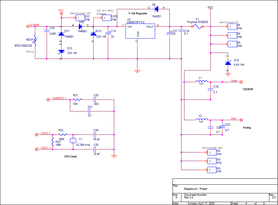
The MegaSquirt-II PCB receives electrical current along from the vehicle's battery. If the voltage from the charging system surges or spikes (rises above the accepted level) the Metal Oxide Varistor (MOV) diverts just enough current into the outlet's grounding wire to keep the voltage supply to the components at the acceptable level.
A MOV forms a connection between the hot power line and the grounding line. A MOV has three parts: a piece of metal oxide material in the middle, joined to the power and grounding line by two semiconductors.
These semiconductors have a variable resistance that is dependent on voltage. When voltage is below a certain level, the electrons in the semiconductors flow in such a way as to create a very high resistance. When the voltage exceeds that level, the electrons behave differently, creating a much lower resistance to ground. When the voltage is correct, an MOV does nothing. When voltage is too high, an MOV can conduct 'excess' current to ground in order to eliminate the extra voltage.
Because the extra current is diverted into the MOV and to ground, the voltage in the PCB power supply line returns to a normal level, so the MOV's 'by-pass' resistance shoots up again. In this way, the MOV only diverts the surge current, while allowing the standard current to continue powering the components on the PCB.
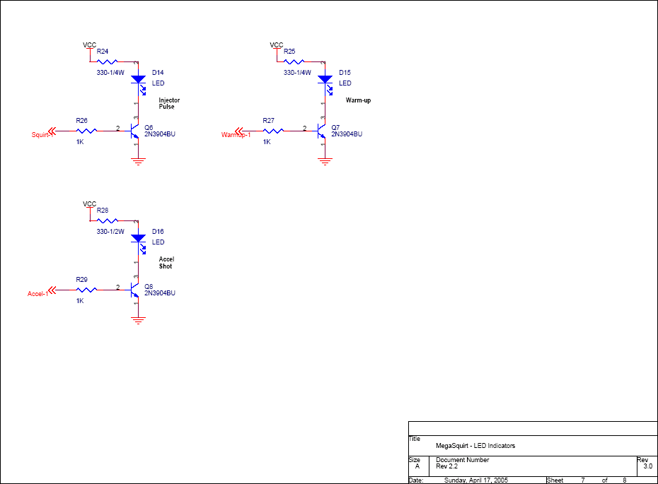
MegaSquirt v3.0 PCB Schematics
Please note that a few component values may have been tweaked - especially in the VR input circuit, but possibly others as well. Follow the BOM values for the current component specifications and use these over the values listed on the following schematics.

Note 1: For MS-II daughter card implementation, the following signals apply to DIP-40 socket:

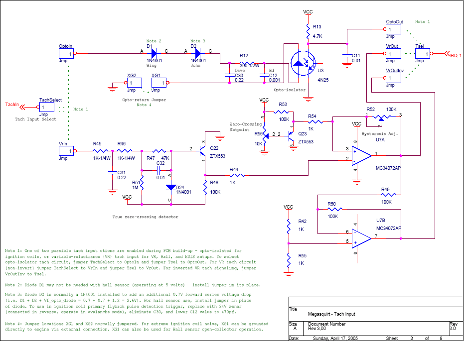
Note 1: One of two possible tach input options are enabled during PCB build-up:
To select opto-isolator tach circuit, jumper TachSelect to OptoIn and jumper Tsel to OptoOut. For VR tach circuit (non-invert) jumper TachSelect to VrIn and jumper Tsel to VrOut. For inverted VR tach signaling, jumper VrOutInv to Tsel.
Note 2: Diode D1 may not be needed with Hall sensor (operating at 5 volts) - install jumper in its place.
Note 3: Diode D2 is normally a 1N4001 installed to add an additional 0.7V forward series voltage drop (i.e. D1 + D2 + Vf_opto_diode = 0.7 + 0.7 + 1.2 = 2.6V). For Hall sensor use, install jumper in place of diode. To use in ignition coil primary flyback pulse detection trigger, replace with 24V Zener (connected in reverse, operate in avalanche mode), eliminate C30, and lower C12 value to 470 pF.
Note 4: Jumper locations XG1 and XG2 normally jumpered. For extreme ignition coil noise, XG1 can be grounded directly to engine via external connection. XG1 can also be used for Hall sensor open-collector operation.
Please note that a few component values may have been tweaked - especially in the VR input circuit, but possibly others as well. Follow the BOM values for the current component specifications and use these over the values listed on the following schematics.
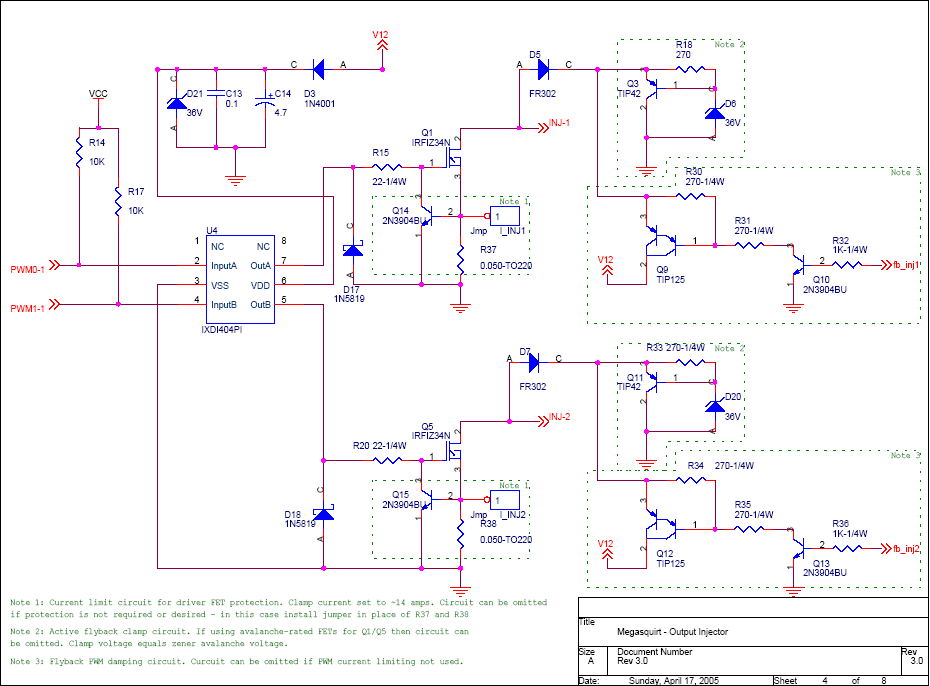
Note 1: Current limit circuit for driver FET protection. Clamp current set to ~14 amps. Circuit can be omitted if protection is not required or desired - in this case install jumper in place of R37 and R38
Note 2: Active flyback clamp circuit. If using avalanche-rated FETs for Q1/Q5 then circuit can be omitted. Clamp voltage equals Zener avalanche voltage.
Note 3: Flyback PWM damping circuit. Circuit can be omitted if PWM current limiting not used.
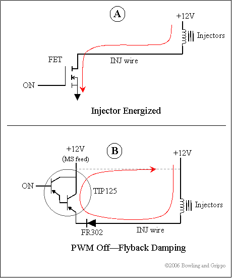
The top drawing A shows the current when the injector driver is on, during the high-time of the PWM waveform. Basically the FET is turned on, energizing the injector. This is the PWM high time, and it depends on the setting of the PWM duty cycle.
The second drawing B is the path when the driver is turned off during PWM flyback damping, or recirculation mode. This occurs during the off time of the PWM current limit. During this time the injector is trying to maintain the current that was there during the PWM on time (see Lenz law). So the injector will generate a current (from the collapsing magnetic field) that flows thru the FR302 diode, the TIP125 transistor, thru the +12V feed and back to the injector. The +12V feed to the MS is used as a path. Note that this is the closed loop path, this is not ground-referenced - the +12V is used as a return path, not as the potential source.
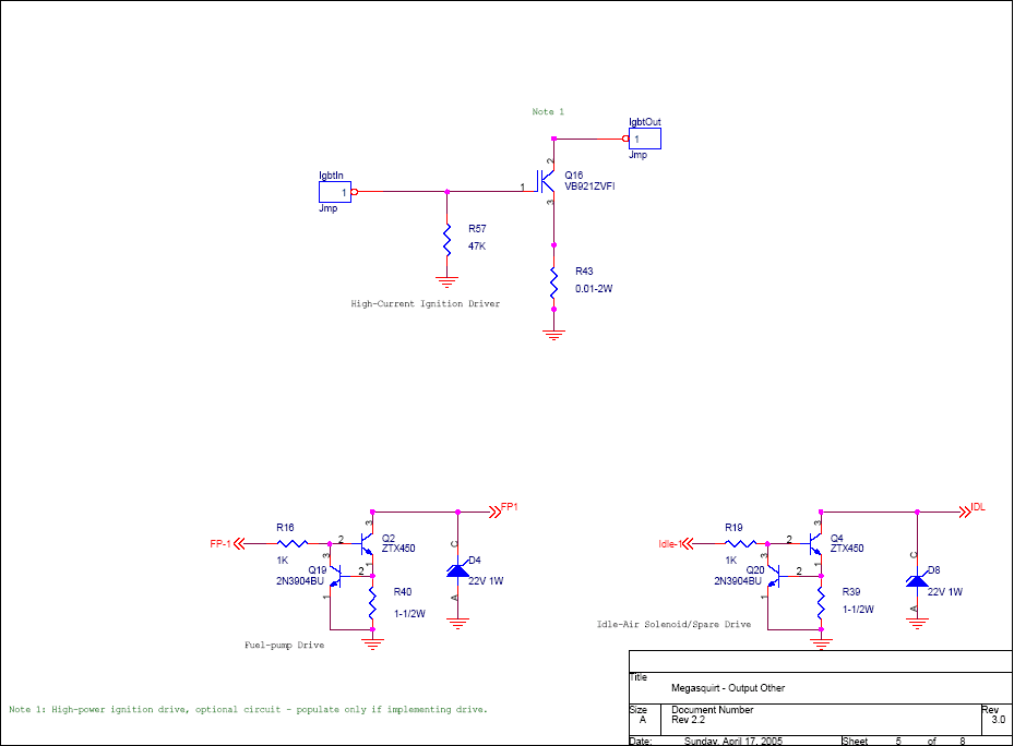
Note 1: High-power ignition drive, optional circuit - populate only if implementing drive.
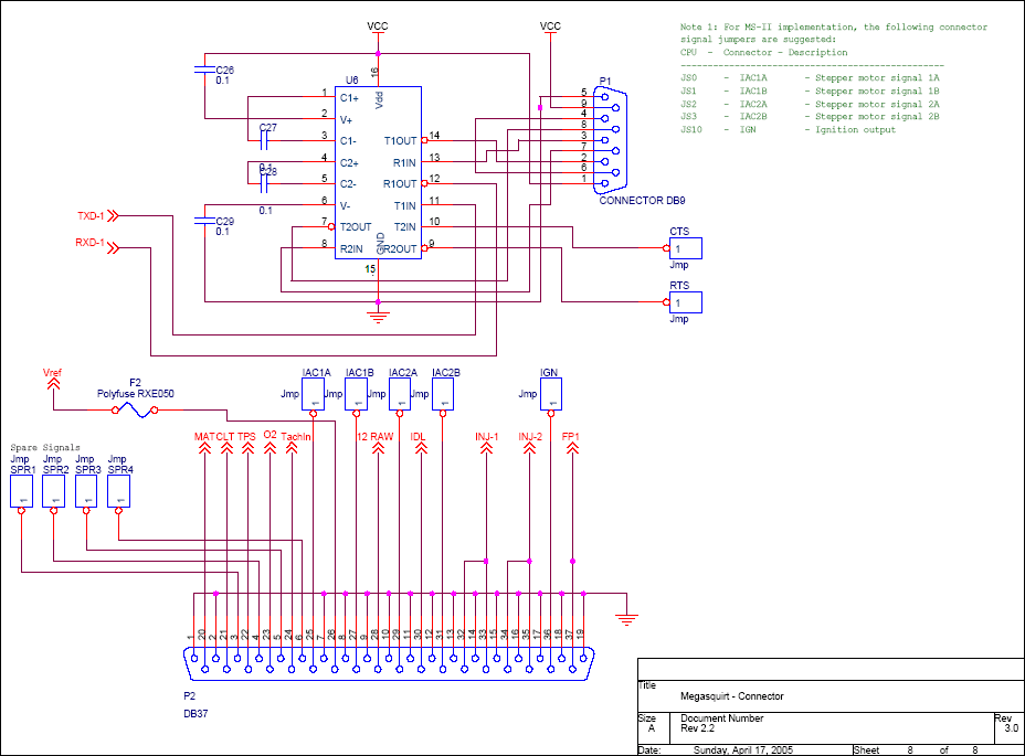
Note 1: For MS-II implementation, the following connector signal jumpers are suggested:
| CPU | Connector | Description |
| JS0 | IAC1A | Stepper motor signal 1A |
| JS1 | IAC1B | Stepper motor signal 1B |
| JS2 | IAC2A | Stepper motor signal 2A |
| JS3 | IAC2B | Stepper motor signal 2B |
| JS10 | IGN or IGBTIN (w/ IGBTOUT->IGN) check manual | Ignition output |
| JS6 | SPR1/CANH | CAN High |
| JS8 | SPR2/CANL | CAN Low |